Things don't look too good for semiconductor equipment companies in 2009. The worst projections come from Gartner: semiconductor equipment spending is projected to decline 30.6 percent in 2008 and another 31.7 percent in 2009, according to a revised forecast issued Dec. 18. On October 8, Gartner projected that equipment spending would decline 25.2 percent in 2008 and 8.9 percent in 2009.
I use the term worst to signify the greatest drops, even though I fail to understand how a company can give forecasts in tenths of decimal places only to change it two months later again in tenths of decimals. Why don't they just say about 25% or about 9%. Does the tenth of decimal forecast give credibility or make it look sort of foolish?
How bad can it get for semiconductor equipment manufacturers going forward? Consider this. How about if companies ranked 21 and below all of a sudden are forced out of business and only the top 20 remain? This could happen if the proposals set about for 450mm wafers come into play. Let me explain.
Periodically silicon wafers get bigger. Historically, wafers have increased a generation every 2-4 years, or about 25mm per year, as shown in the table below.
Year |
Inches |
MM |
1960 |
0.525 |
13.3 |
1964 |
1 |
25.4 |
1966 |
1.5 |
38.1 |
1970 |
2.25 |
57.2 (50) |
1973 |
3 |
76.2 (75) |
1975 |
4 |
101.6 (100) |
1979 |
5 |
127.0 (125) |
1981 |
6 |
152.4 (150) |
1985 |
8 |
203.2 (200) |
1998 |
12 |
304.8 (300) |
Manufacturing with larger wafers helps increase the ability to produce semiconductors at a lower cost. The total silicon surface area of a 450mm wafer and the number of printed die (individual computer chips, for example) is more than twice that of a 300mm wafer.
Cost to the IC equipment industry can reach as high as $100 billion to develop 450mm tools. Only a few chipmakers—Intel (INTC), Samsung (SSDIF.PK) and possibly Toshiba (TOSBY.PK) and TSMC (TSM)—can afford to build 450mm fabs, which could cost $10 billion or more. In fact, on May 5, 2008, Intel, Samsung, and TSMC announced they reached agreement on the need for industry-wide collaboration to target a transition to larger, 450mm-sized wafers starting in 2012.
It appears that these three companies have taken the steps to championing the cause. While Intel backed the conversion to 150mm wafers and IBM supported the 200mm wafer conversion, Applied Materials (AMAT) took it upon itself to foster conversion to 300mm by internally funding development of a full suite of 300mm tools. Faced with the task of competing with Applied on this level, competitors rushed to develop their own tools. Industry consortia such as I300I and SELETE did not pay any development costs, leaving the entire 300mm wafer conversion to the equipment vendors.
Both the semiconductor and equipment industries prior to 2001 worked in tandem in a cyclical fashion of peaks and valleys every 2 years or so as shown below.
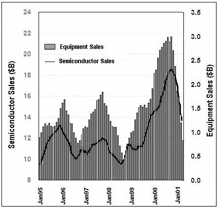
After 2001, the industry changed, and the semiconductor industry continued a relentless growth while the equipment industry has been relatively flat, save for the peaks and valleys reminiscent of the 90s.
In 2002, 1.4% of silicon wafers processed were 300mm in diameter. In 2008, 37.4% were 300mm. Within that time, semiconductor revenues increased from about $10 billion per month at the start of 2002 to $20+ billion in December 2008. In contrast, semiconductor equipment bookings started off 2002 at $645 million, reached a peak of $1.8 billion in June 2006, and ended 2008 at about $800 million. Quite a disconnect! If you want a chart from Jan 1995 to the end of 2008, which clearly illustrates these trends, go to my web site at www.theinformationnet.com, click on the "contact us" button, and we will send you the gif file by e-mail.
The semiconductor industry is pushing hard for 450mm wafers because it will reduce costs. While the migration to 450 will not happen overnight, the largest IC manufacturers, who are the largest equipment buyers, will be manufacturing ICs by the middle of the next decade on these wafers. True 6 years is a long time on Wall Street, but by that time we will start to see the largest equipment companies get larger, but IC equipment companies are small to midsized operations with limited R&D budgets and they will go out of business.